APCCAS 2025 invites all attendees, especially students, to participate in our tutorials. Through the Continuing Education initiative, you can gain exclusive IEEE credentials. This opportunity is designed to enhance tutorials’ value, participation, and quality, providing an enriching educational experience for all.
By attending, youŌĆÖll receive an official IEEE certificate with Continuing Education Units (CEUs) or Professional Development Hours (PDHs), offering recognized validation of your commitment to continuous learning.
Why Participate?
- Recognition and Credibility
Enhance your professional qualifications with IEEE-certified credentials, formally recognizing your commitment to lifelong learning. Attendees can add these qualifications to their academic or professional profiles, increasing credibility and distinction in their field. - Boosting Participation Value
As part of the Continuing Education initiative, these tutorials offer extra value beyond standard conference experiences, making them an excellent opportunity for students and professionals alike. - Elevated Tutorial Quality
All tutorials are held to rigorous standards to qualify for IEEE credentials, ensuring high-quality content and a rewarding learning experience./li> - Align with IEEE’s Esteemed Recognition
Gain IEEE-branded certification, a mark of excellence, that aligns your learning with IEEEŌĆÖs globally respected reputation./li>
Whether you are looking to broaden your expertise, gain industry-recognized certification, or connect with peers, the APCCAS 2025 tutorials provide a platform to elevate your professional development and align with IEEEŌĆÖs Continuing Education standards. DonŌĆÖt miss this chance to invest in your future.
 |
Designing compact SoC PWM switched-inductor power suppliesGabriel A. Rinc├│n-Mora |
|
Biography
Gabriel A. Rinc├│n-Mora is Motorola Solutions Foundation Professor, Fellow of the National Academy of Inventors, Fellow of the IEEE, and Fellow of the Institution of Engineering and Technology. He was with Texas Instruments in 1994ŌĆō2004 and has been with the Georgia Institute of Technology since 1999. He’s received the IEEE Charles A. Desoer Technical Achievement Award, Distinguished Faculty Achievement Award, IEEE Joseph M. Biedenbach Outstanding Engineering Educator Award, IEEE Outstanding Educator Award, Charles E. Perry Visionary Award, Three-Year Patent Award, National Hispanic in Technology Award, Orgullo Hispano Award, Hispanic Heritage Award, State of California Commendation Certificate, and IEEE Service Award. His body of work includes 4 textbooks, 5 slide books, 3 literary books, 8 handbooks, 4 book chapters, 44 patents, over 200 articles, over 26 commercial power-chip products released to production, 25 educational videos, and over 170 keynote addresses, distinguished lectures, and research seminars. Abstract
Switched-inductor power supplies are pervasive in electronics. This is because they deliver a large fraction of the power they draw from the input source with an output current or voltage that is largely independent of the load. Keeping the output current or voltage steady this way is ultimately the responsibility of the feedback controller. This |
|
 |
Overcoming the Transimpedance Limit: On the Design of Low-Noise TIADan Li |
|
Biography
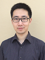
Dan Li received the B.E. and M.E. degrees from Northwestern Polytechnical University, XiŌĆÖan, in 2004 and 2007, respectively, and the Ph.D. degree from the University of Pavia, Pavia, Italy, in 2013. From 2007 to 2009, he worked at the Nvidia Shanghai R&D Center, where he focused on custom SRAM circuit design. From 2011 to 2014, he was with the Studio di Microelettronica, STMicroelectronics, Pavia, Italy, working on CMOS optical receivers for 100 GbE optical links and silicon photonics applications. He joined XiŌĆÖan Jiaotong University, XiŌĆÖan, in 2015, where he currently serves as a professor. His current research interests include high-speed optical interconnects, 3D sensing, and low-power mixed-signal circuits. He has served as Track Chair (Wireline) and TPC Member of IEEE ICTA, Publicity Chair of IEEE ICECS 2020, Sponsorship/Exhibition Chair of IEEE ICTA 2022, and Local Arrangement Chair of IEEE BioCAS 2024. Abstract
With the mass deployment of optical links to meet the ever-increasing communication bandwidth demands from data communication and AI, there is a growing need for low-cost components. Furthermore, the advent of Co-Packaged Optics (CPO)ŌĆöwhere electronics and photonics are integrated into a single packageŌĆöwill further drive improvements in bandwidth density and power efficiency. In this context, integrated solutions are not only desirable but often essential, leading to the adoption of silicon photonics and CMOS-based electronics, replacing the traditional dominance of III-V optics and SiGe electronics. |
|
 |
Short-Length ECC Decoders: Design Challenges for Future URLLC SystemsYoungjoo Lee |
|
Biography
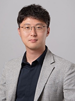
Youngjoo Lee received the B.S., M.S., and Ph.D. degrees in Electrical Engineering from the Korea Advanced Institute of Science and Technology (KAIST), Daejeon, South Korea, in 2008, 2010, and 2014, respectively. Since 2025, he has been with the School of Electrical Engineering at KAIST, where he is currently an Associate Professor. Prior to joining KAIST, he was with the Interuniversity Microelectronics Center (IMEC), Leuven, Belgium, from 2014 to 2015, where he worked on reconfigurable SoC platforms for software-defined radio systems. He was an Assistant Professor in the Department of Electronic Engineering at Kwangwoon University, Seoul, South Korea, from 2015 to 2017. From 2017 to 2025, he served as a faculty member in the Department of Electrical Engineering at Pohang University of Science and Technology (POSTECH), Pohang, South Korea. His current research interests include algorithm-hardware co-design for application-specific processors, energy-efficient machine learning accelerators, advanced error correction codes, and next-generation wireless systems. More information is available at: https://sites.google.com/view/epiclab Abstract
As 5G advances and 6G approaches, ultra reliable low latency communication (URLLC) is becoming increasingly important in next generation wireless systems. The growing presence of intelligent applications such as autonomous systems, real time control, and on device AI has led to a rapid increase in the demand for fast and reliable transmission of short data packets. This shift brings new and significant challenges to error correction coding, especially in terms of decoding performance, latency, throughput, and energy efficiency. Short length ECC decoders, unlike those designed for longer codes, face unique design constraints due to limited redundancy and tighter timing requirements. Traditional approaches are often insufficient in these scenarios. In this tutorial, we will examine the key challenges in designing ECC decoders for URLLC applications using short codes. We will first explore how existing polar decoders, currently used in 5G systems, can be optimized for improved performance in short packet communication. In addition, we will discuss emerging ECC schemes that aim to replace the current 5G polar codes. We will highlight important considerations in decoder implementation for these new codes and compare their strengths and weaknesses against standard polar decoders |
|
 |
Advanced Techniques for High Efficiency Oversampling Data Converters from Discrete-Time to Continuous-Time: Fundamentals, Recent Trends, and Perspectives Sai-Weng Sin, Terry |
|
Biography
Sai-Weng Sin is currently a Professor with the Dept. of ECE, Faculty of Science and Technology, and the Deputy Director (Academic) of the Institute of Microelectronics, as well as the Deputy Director of State-Key Laboratory of Analog and Mixed-Signal VLSI, University of Macau. Abstract
High efficiency oversampling data converters have become increasingly popular and significant in the various emerging applications, ranging from the data acquisition in IoT sensor nodes that demands an ultra-high resolution with very low power consumption to wideband wireless communications in medium/high resolution. |
|
 |
Liang Qi |
|
Biography
Liang Qi (Senior Member, IEEE) received B.Sc. degree from Xidian University, China, in 2012 and Ph.D. degree from University of Macau, Macao, China, in 2019. |
|
 |
SPAD-Based Solid-State LiDAR in CMOS: From Fundamentals to State-of-the-Art IntegrationSeong-Jin Kim |
|
Biography
Seong-Jin Kim received his B.S. degree in electrical engineering from the Pohang University of Science and Technology, Pohang, South Korea, in 2001, and M.S. and Ph.D. degrees in electrical engineering from KAIST, Daejeon, South Korea, in 2003 and 2008, respectively. Abstract
This tutorial will present a comprehensive overview of the enabling technologies behind single-photon avalanche diode (SPAD)-based solid-state CMOS LiDAR sensors that have emerged as a key component in autonomous vehicles and immersive mobile applications such as augmented and virtual realities (AR/VR). It will begin with an introduction to the fundamental principles of both direct and indirect time-of-flight (ToF) techniques. Subsequently, the tutorial will delve into the three core building blocks of a SPAD-based LiDAR system: (1) SPAD devices and analog front-end circuit to enable photon-level sensitivity; (2) time-to-digital converters (TDC) to translate photon arrival times into precise temporal measurements; and (3) histogram-based signal processing units to reconstruct depth information from stochastic photon detections. The session will finally explore recent advances in fully integrated on-chip histogramming TDC architectures, highlighting selected state-of-the-art implementations. |
|